— Industry’s First Double-Sided and Internal Defect Inspection —
YOKOHAMA, JAPAN -
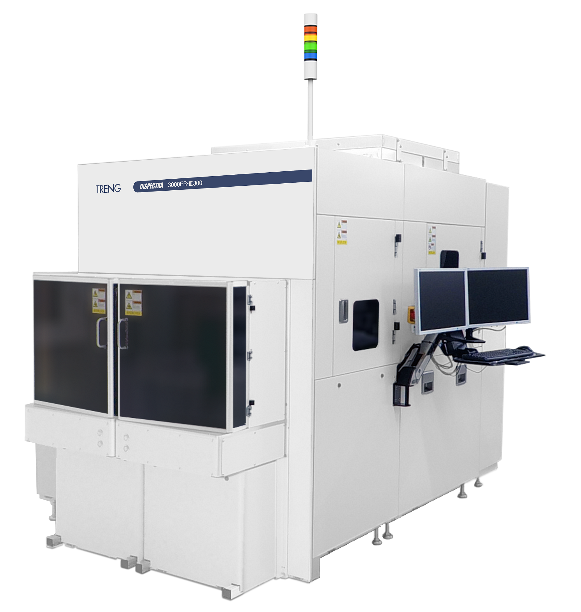
Media OutReach Newswire - 27 February 2025 - TASMIT Inc. has launched a new inspection system for glass substrates as part of its INSPECTRA® series of semiconductor wafer visual inspection systems, which has gained attention for its high efficiency in advanced semiconductor manufacturing.
Read more: TASMIT Launches Large Glass Substrate Inspection System for Advanced Semiconductor Packaging